Designing the bootstrap supply for a high-side gate driver
The bootstrap capacitor, diode and resistor look like three trivial parts, yet they decide maximum duty cycle, start-up behaviour and whether the high-side MOSFET ever sees a weak gate. How to size them with numbers.
Why a high-side switch needs its own supply
An N-channel MOSFET turns on when its gate is about 10 V (its operating V_GS) above its source. For the low-side switch the source is ground, so the driver's 12 V supply (V_CC) does the job. For the high-side switch the source is the switch node (VS), which swings between 0 V and the full bus voltage (V_BUS). With the switch on, the gate has to sit at bus voltage + 10 V.
The bootstrap circuit is the cheapest way to get there. Three parts do it:
- Bootstrap capacitor
C_BOOTbetween the driver's floating supply pin (VB) and the switch node (VS). It is the high-side driver's rechargeable battery. - Bootstrap diode
D_BOOTfrom the 12 V supply (V_CC) toVB. - Bootstrap resistor
R_BOOT(optional, but recommended) in series with the diode, to limit the charging and inrush current.
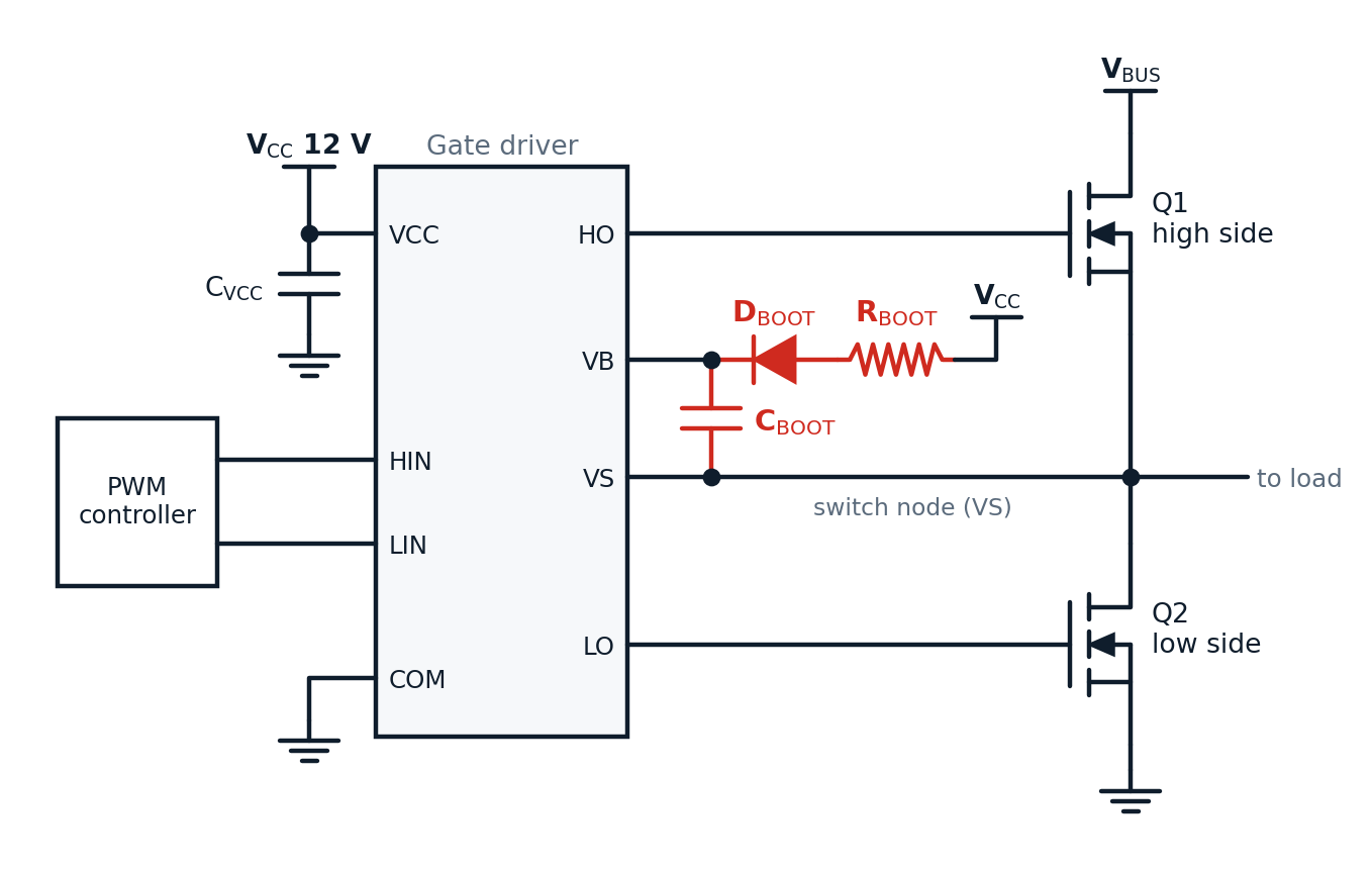
When the low-side switch is on, VS sits near ground and C_BOOT charges through the diode to about V_CC − V_F. When the high-side switch turns on, VS rises to the bus voltage, the diode blocks, and C_BOOT rides up with it. The driver now has V_CC − V_F between VB and VS to drive the gate.
The catch: C_BOOT only recharges while the low-side switch is on. Everything the high side consumes in between comes out of that one capacitor.
Step 1: add up the charge
During each high-side on-time, C_BOOT supplies:
| Charge | Expression | What it is |
|---|---|---|
| Gate charge | Q_G | Charge to turn the MOSFET on, from the datasheet at your V_GS |
| Driver quiescent | I_QBS · t_on(max) | High-side section's own supply current |
| Level shifter | Q_LS | Charge per cycle for the level-shift stage (driver datasheet, a few nC) |
| Gate pull-down | (V_GS / R_GS) · t_on(max) | Current through any gate-source resistor |
| Leakage | (I_LK,C + I_R,D) · t_on(max) | Capacitor leakage and diode reverse leakage (hot) |
Q_TOTAL = Q_G + Q_LS + (I_QBS + V_GS/R_GS + I_LK) · t_on(max)
Use the longest high-side on-time the system can command: the highest duty cycle at the lowest switching frequency. In a motor drive that can be a full PWM period or longer during low-speed, high-torque operation.
Step 2: choose the allowed droop
The capacitor voltage drops by ΔV = Q_TOTAL / C_BOOT during the on-time. The floor is set by two limits:
- The driver's high-side under-voltage lock-out (
V_BS UVLO, often 8–9 V). Below it, the driver switches the high side off on its own. - The gate voltage the MOSFET needs for its rated on-resistance, usually 10 V. Above the UVLO, a weak gate still means a hot MOSFET.
C_BOOT ≥ Q_TOTAL / ΔV_allowed
Pick an allowed droop well inside that window (0.5 V is a good target), then add margin for capacitor tolerance and DC-bias derating. A ceramic X7R capacitor can lose 30–60 % of its capacitance at its working voltage, depending on case size and rating. Although VS swings up to the bus voltage, C_BOOT itself only ever sees about V_CC (12 V) across its terminals, so a 25 V or 50 V part keeps the DC-bias loss small.
Worked example
Illustrative values: a 100 V MOSFET switched at 20 kHz, 12 V driver supply, duty cycle up to 95 %, 0.5 µs dead-time on each edge.
| Parameter | Value |
|---|---|
Q_G at 12 V | 60 nC |
Q_LS | 5 nC |
I_QBS (max) | 100 µA |
Gate pull-down R_GS | 47 kΩ |
t_on(max) | 0.95 / 20 kHz = 47.5 µs |
Dead-time t_dead | 0.5 µs per edge |
V_F of bootstrap diode | 0.7 V |
The charge:
- Gate: 60 nC
- Level shifter: 5 nC
- Driver quiescent:
100 µA × 47.5 µs= 4.8 nC - Gate pull-down:
(11.3 V / 47 kΩ) × 47.5 µs = 0.24 mA × 47.5 µs= 11.4 nC - Total ≈ 81 nC; use 82 nC (rounded up, or the pull-down taken at the full 12 V)
The capacitor charges to about 12 − 0.7 = 11.3 V. For an allowed droop of 0.5 V:
C_BOOT(min) ≥ 82 nC / 0.5 V = 164 nF
Allowing ×3 for tolerance, ageing and DC-bias derating gives about 0.5 µF *effective* minimum. A 1 µF, 25 V or 50 V X7R capacitor in 0805 typically still provides 0.6 µF or more at 11.3 V bias, so it fits. With 0.6 µF effective installed, the actual droop each cycle is only ΔV = 82 nC / 0.6 µF ≈ 0.14 V.
Rule of thumb for the 12 V side: the driver's V_CC decoupling capacitor should be at least 10× C_BOOT, here 10 µF. Every recharge pulls a step of charge out of it, and you don't want V_CC dipping by the same amount.
Step 3: check the recharge time and the maximum duty cycle
C_BOOT only refills while the low-side switch is actually conducting. With D the high-side duty cycle and a dead-time on both edges of the low-side pulse:
t_L = (1 − D) / f_sw − 2 · t_dead
At high duty cycle the dead-time takes a large bite out of this window. The recharge path is R_BOOT, the diode's dynamic resistance and the low-side MOSFET:
τ = (R_BOOT + R_D + R_DS(on),LS) · C_BOOT ≈ (R_BOOT + R_D) · C_BOOT
The capacitor does not need to refill completely from empty every cycle. It only has to put back the small droop ΔV. When t_L is short compared with τ, part of the droop is left over, and the capacitor settles at a lower voltage where each recharge exactly replaces each discharge. That steady-state shortfall is:
V_short = ΔV · e^(−t_L/τ) / (1 − e^(−t_L/τ))
and the lowest voltage the high-side driver ever sees is:
V_BS(min) = V_CC − V_F − V_short − ΔV
For the example at 95 % duty: t_L = 2.5 µs − 2 × 0.5 µs = 1.5 µs, 0.6 µF effective, R_D ≈ 1 Ω and the actual droop ΔV = 0.14 V:
R_BOOT | τ | Shortfall | V_BS(min) | First-charge peak current |
|---|---|---|---|---|
| 10 Ω | 6.6 µs | 0.55 V | 10.6 V | 1.0 A |
| 4.7 Ω | 3.4 µs | 0.25 V | 10.9 V | 2.0 A |
| 2.2 Ω | 1.9 µs | 0.12 V | 11.0 V | 3.5 A |
A smaller R_BOOT keeps the gate voltage up at high duty cycle, but the first charge of an empty capacitor then draws a large peak current through the diode and the low-side switch: (V_CC − V_F) / (R_BOOT + R_D).
All three values clear the 10 V target here, and 10 Ω does it with the lowest start-up peak. The catch is how little margin it leaves: 0.6 V above the target, with the capacitor at its nominal derated value. A capacitor at the low end of its tolerance, hot diode leakage or a longer dead-time each eat into that. 4.7 Ω buys another 0.3 V for a 2 A start-up peak, which is the choice we would make. Either way, use a pulse-rated resistor (0805 or 1206) to withstand repeated pre-charge pulses, and check the diode's surge rating.
100 % duty is impossible with a plain bootstrap: with the low side never on, the capacitor never refills. A drive that must hold the high side on indefinitely needs a charge pump or an isolated high-side supply. Many controllers simply enforce a minimum low-side pulse every cycle.
Step 4: charge it before the first pulse
At power-up C_BOOT is empty. If the controller's first command is a high-side pulse, the driver's UVLO keeps the high side off, or worse, turns it on weakly.
- Pre-charge by turning the low-side switch on briefly before switching starts, for a few τ (typically 20–50 µs). In a three-phase motor drive with the rotor stationary, pulse all three low sides together: there is no phase-to-phase voltage, so no stator current flows.
- After a long idle or fault, repeat the pre-charge: leakage drains the capacitor.
- Caution with a spinning motor (flying restart): turning on all three low sides at once short-circuits the windings against the back-EMF. That is dynamic braking, with a sharp torque jolt and large phase currents. Instead, let the low-side body diodes recharge
C_BOOTas each switch node swings low during free-wheeling, pulse one leg at a time with current limiting, or use a charge pump.
Step 5: choose the diode
- Voltage rating: at least
V_BUS(max), plus 20–30 % margin for switch-node overshoot. TheVBpin swings toV_BUS + V_CCrelative to ground, but the diode's own reverse voltage is onlyVB − V_CC ≈ V_BUS. - Fast recovery: use an ultra-fast (
t_rr< 35 ns) or Schottky diode. When the high side turns on, a slow diode conducts in reverse for its recovery time, dragging charge out ofC_BOOTand injecting high-frequency ringing. - Schottky caution: reverse leakage rises exponentially with temperature and drains
C_BOOTfor the whole on-time. Check the leakage at maximum junction temperature and include it in Step 1. - Internal diodes: many drivers have a bootstrap diode or switch built in, but it often has 20–40 Ω of internal resistance. An external Schottky in parallel recharges much faster at high duty cycle.
Step 6: protect against switch-node undershoot
When the high-side switch turns off with load current flowing, the current moves to the low-side body diode. Parasitic inductance in that loop forces VS below ground for a few nanoseconds, by L · di/dt, often 5–10 V or more on a fast, high-current stage.
Two things go wrong:
- Over-charging: with
VSnegative, the bootstrap diode chargesC_BOOTbeyondV_CC.VB − VScan easily exceed the driver's absolute maximum rating (for example 12 V − (−6 V) = 18 V). - Driver upset: large negative
VScan disturb the level shifter or latch some drivers.
Fixes:
- Keep the power loop small, and connect the driver's
VSandCOMclose to the MOSFET source pins, not after a length of high-current copper. - Add a small damping resistor (a few ohms) between the switch node and the driver's
VSpin, and a Schottky clamp fromCOMtoVS(anode toCOM, cathode toVS) right at the driver pins. - Connect
C_BOOTdirectly across the driver'sVBandVSpins, on the driver side of that damping resistor, with no vias in the loop if possible. - Check the driver's negative
VStransient rating and itsdV_S/dtlimit.
Design checklist
- Add up the total high-side charge per cycle: gate, level shift, quiescent, pull-down and hot leakage, at the longest on-time.
- Set the droop from the high-side UVLO and the MOSFET's required gate voltage, not from the gate charge alone.
- Derate ceramic capacitance for DC bias. Size for the *effective* value.
- Make the
V_CCdecoupling at least 10×C_BOOT. - Check recharge at the highest duty cycle with the steady-state shortfall formula, dead-time included, and choose a pulse-rated
R_BOOT. Use a charge pump if you need 100 % duty. - Pre-charge before the first high-side pulse (only with the rotor stationary in a motor drive), and after long idle periods.
- Pick a fast diode rated for
V_BUSplus ringing margin, and check its hot reverse leakage. - Protect against negative
VSundershoot: tight layout,C_BOOTright at the driver pins, a series damping resistor and a Schottky clamp. - Measure
VB − VSon the bench at maximum duty, minimum frequency and maximum temperature.
Need a hand with a gate-drive design?
IDEAS designs gate drives, motor controllers and power converters, from component sizing to layout and bench validation. If a high-side switch runs hot or drops out at high duty cycle, talk to us.
Talk to the IDEAS team about your hardware or firmware.